|
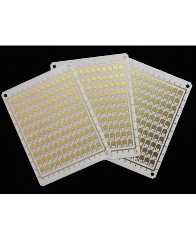
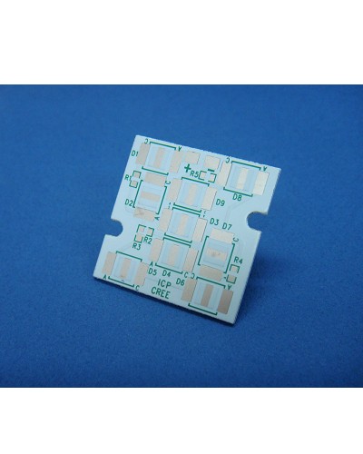
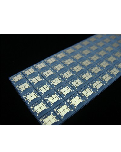
璦司柏電子股份有限公司(簡稱ICP)成立於2009年6月,位於桃園縣龜山鄉,為國內第一個將半導體製程與設備整合入以氧化鋁/氮化鋁為基版之被動/保護元件之研發團隊。主要的營運項目為精密電子陶瓷之線路設計製造;是一群研發團隊為實現理想而創立的公司,擁有獨特且先進的研發與製程能力。 ICP 電子研發團隊已歷經10年的薄膜元件開發經驗,於今年10月完成第三代薄膜專業代工之生產線,結合元件/微線路設計、真空沉積、曝光顯影與電鍍/化學鍍沉積等技術,ICP能提供各式陶瓷基板金屬化設計加工與薄膜型被動/保護元件整合設計製造。薄膜製程能精確控制元件線路設計(線寬與膜厚),厚膜製程能提供散熱途徑與耐候條件。舉凡:陶瓷/矽基板金屬化設計加工、LED陶瓷散熱基版薄膜製程加工、覆晶封裝基板設計製造、薄膜/厚膜/電鍍/無電鍍製程整合設計加工與薄膜型被動元件整合設計製造皆為我司所能提供之服務。
Established in Jun 2009 and located in Taoyuan. ICP is dedicated to apply the thin film & lithography process on Alumina/Aluminium Nitride substrate to make passive and circuit components. With both circuit design and processing capabilities, ICP can offer OEM/ODM manufacturing service for products with circuits on ceramic substrate. With over 10 years of thin film components developing experience, The team members in ICP have already set up the 3rd generation OEM/ODM manufacturing service line. The line combines vacuum thin film deposition, lithography processing, electrodeposition and chemical deposition. ICP can provide design and manufacturing services including, LED heat sink substrate , thin film passive/circuit protection integrated components, metallization of ceramic/silicon substrate, flip chip package substrate and thin/ thick film/ electro-deposition/ electroless-deposition integration processing.
|